



Semiconductor: Sand to Chip solutions
Wafer fabrication,advance packaging & inspection equipments for R&D and Industry.
Material Science & Wet Processes
Thin-film deposition and wet surface chemistry equipments
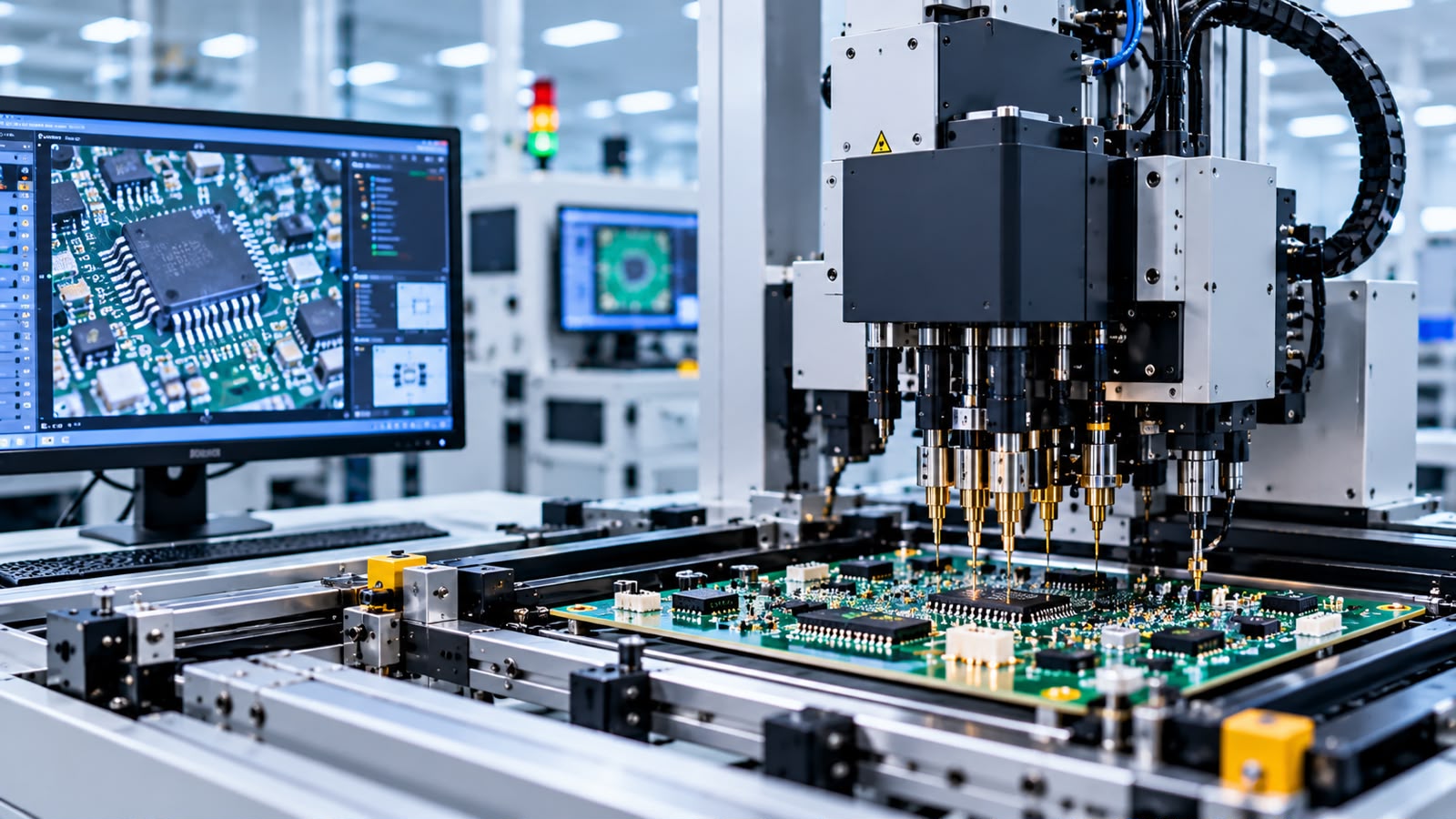
IVS(Inspection vision system)
3D Automated Optical Inspection (AOI),Solder Paste Inspection(SPI) for SEMI & SMT Industry
What we do
Adam TechPro Private Limited was founded in 2020 and is led by Highly experienced Ph.D professionals from Semicon and Material Science industry along with directors Jatin Ruparelia and Arya Dalvi, providing advanced scientific and industrial solutions in the fields of Photonics, Semiconductor, Nanotechnology, Quantum, MEMS Technology, and Material Science, to name a few. It was established with a vision to connect the Indian scientific and manufacturing community with cutting-edge technology from around the world, tailored to their specific needs. Adam TechPro offer smooth gateway to foreign manufacturers of pioneering technologies, with unmatched service, valuable expertise, and experiential insight into the market.
01
Semiconductor Solutions
Wafer Fabrication, Advanced Packaging, and Inspection equipment for R&D, and Industrial Applications.
02
Thin-Film Deposition
Thin Film Deposition, Ion Beam Etch, PE-CVD, and PIB-CVD systems (including Infinity, Discovery, Voyager, Integrity, Phoenix, Versa, and Research lines) for Semiconductor, Opto-electronics, display, and microanalysis applications (such as sensors, power devices, EUV lithography, IR detectors, lasers, OLED encapsulation, DLC/TCO coatings, and failure analysis).
03
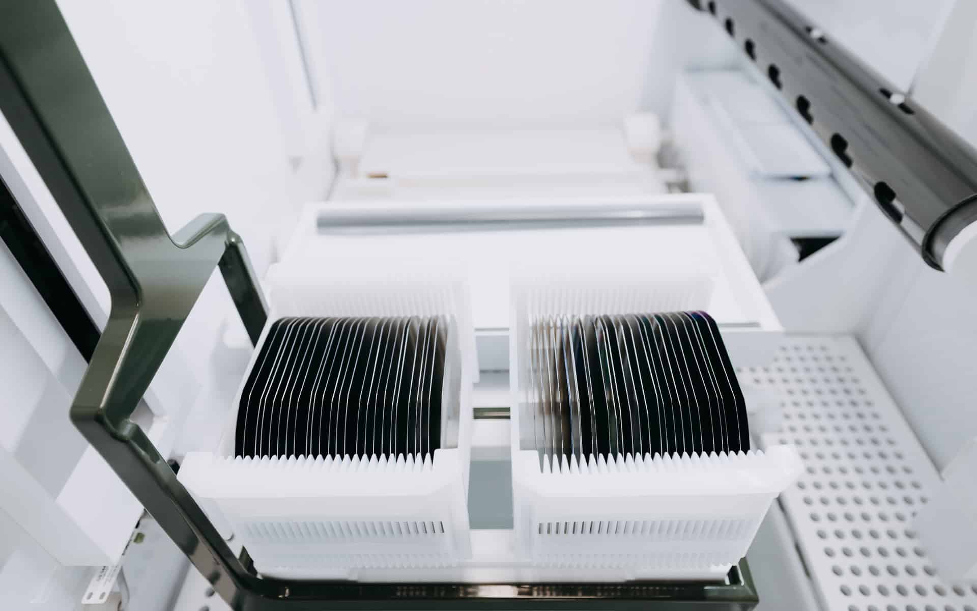
Wet Processing Solutions
Equipment for Automated batch wet benches, single-wafer processing systems, and fab logistics equipment for FEOL/BEOL semiconductor manufacturing, MEMS, microstructuring, and R&D applications, including wafer cleaning, etching, stripping, electroless plating, and lift-off processes
04
Vision & Inspection
Advanced 3D and 2D AOI, SPI, and semiconductor inspection systems for SMT manufacturing, PCB assembly, and advanced packaging applications
OUR SOLUTIONS
Advanced Equipment for Industry
Discover equipment solutions for semiconductor manufacturing, thin-film deposition, wet processing, and electronics inspection. AdamTech brings together specialized technologies for research, development, and industrial applications.
Our Product Categories
Thin-Film Deposition
Wet Processing
Inspection Vision System (IVS)
Semiconductor Solutions
WHY CHOOSE ADAMTECH.
Technology Solutions for Advanced Industries
Specialized Equipment
Explore equipment for semiconductor manufacturing, thin-film deposition, wet processing, and electronics inspection.
Multiple Technology Partners
Thin-Film Deposition solutions from Denton Vacuum (USA) & AP&S(German) for wet processing, alongside inspection and testing equipment.
R&D and Industrial Applications
Explore equipment options for research & development, material science, Semiconductor, Opto-electronics, display, and microanalysis applications (such as sensors, power devices, EUV lithography, IR detectors, lasers, OLED encapsulation, DLC/TCO coatings, and failure analysis)
Latest Insights & Technologies
Explore the technologies, equipment, and applications shaping semiconductor manufacturing, material science, and electronics inspection.

Looking for the Right Equipment for Your Application?
Explore advanced equipment solutions for semiconductor manufacturing, thin-film deposition, wet processing, and Vision & Inspection
. Connect with AdamTech to discuss your application and equipment requirements.